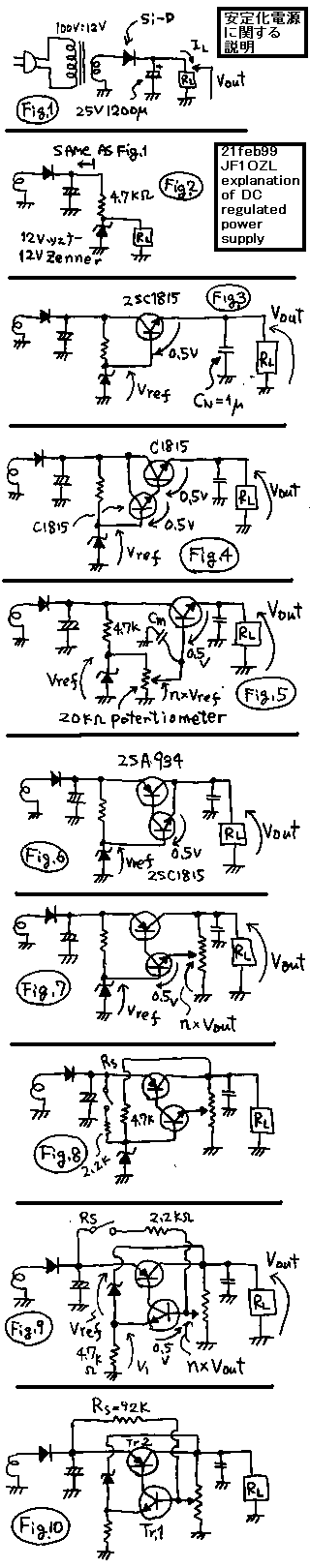
Explanamtion and experiment about regulated DC power supply.......reg.gif
Forward
When I visited the "Douches Museum" in 1996, I looked the "Otto
motor" . That has the automatic speed control system same with the
steam locomotives. In order to get the good knowledge about the inner burn
Engine, it is useful to know about the outer burn Engines. I could learn
many types of the regulated power supply circuits on the electric magazines,
but they were separated image. I gathered them and show you the relation
and performances of each regulator circuits.
| Fig1 |
Rl(ohm) |
Vout(volts) |
Vripple
(volts) |
Nripple(%) |
I(load)( |
Rp(ohms) |
| 0 |
infinite |
17.06 |
0 |
0 |
0 |
- |
| 1 |
150k |
16.70 |
5m |
0.3 |
0.11mA |
3.2k |
| 2 |
4.7k |
16.30 |
60m |
3.68 |
3.46mA |
219 |
| 3 |
300 |
15.47 |
900m |
5.81 |
51.5mA |
30.8 |
Fig1: See fig1! That is non regulated power supply. Such a power supply
was used on the tube radio receiver. The output voltage includes many ripples.
Therefore the tube radio made the sound with many ham noises. In this circuit,
it has some percentage of ripples. Therefore we need to attach the regulator
after this circuit.
These are the definition of some words in this page.
"Rl" is the load resister.
"Vout" is the outlet voltage.
" Vripple" is the voltage of ripple.
"I(load)" is the current of load. It is calculated as I(load)=Vout/Rl.
"Rp" is the inner resistance of this circuit. It is calculated
as Rp=(Vout-V0)/I.
| Fig2 |
Rl(ohm) |
Vout(volts) |
Vripple
(volts) |
Nripple(%) |
I(load)( |
Rp(ohms) |
| 0 |
infinite |
12.17 |
0 |
0 |
0 |
- |
| 1 |
150k |
12.16 |
0 |
0 |
0.081m |
123 |
| 2 |
4.7k |
8.37 |
20m |
2.38 |
1.78m |
2134 |
| 3 |
300 |
12.03 |
5m |
4.85 |
3.43m |
3.24k |
Fig2: Fig2 is regulated by the zenner diode. While the current is small
, this circuit acts good. But because 4.7k ohms of resister is used as
the current supplier for the zenner diode, smaller load than kilo ohms
can not be connected as a load of this circuit.
| Fig3 |
Rl(ohm) |
Vout(volts) |
Vripple(volts) |
Nripple(%) |
I(load)( |
Rp(ohms) |
| 0 |
infinite |
11.67 |
0 |
0 |
0 |
- |
| 1 |
150k |
11.56 |
0 |
0 |
77u |
1.42k |
| 2 |
4.7k |
11.46 |
0 |
0 |
2.44m |
57 |
| 3 |
300 |
11.38 |
5m |
0.439 |
37.9m |
7.65 |
Fig3: Fig3 is the circuit added the transistor emitter follower on the
Fig2. In this circuit, The transistor works as a current amplifier. Vref
is a reference voltage made by the zenner diode. Output voltage becomes
0.5V lower than Vref. When Vout is 37mA, voltage drop becomes 0.3V and
ripple voltage becomes 5mV. This circuit can be used on the power supply
of the small audio amplifier.
| Fig4 |
Rl(ohm) |
Vout(volts) |
Vripple
(volts) |
Nripple(%) |
I(load)( |
Rp(ohms) |
| 0 |
infinite |
11.320 |
0 |
0 |
0 |
- |
| 1 |
150k |
11.11 |
0 |
0 |
74u |
2.8k |
| 2 |
4.7k |
10.93 |
0 |
0 |
2.32m |
168 |
| 3 |
300 |
10.79 |
3m |
0.278 |
36m |
14.7 |
Fig4: Fig3 is the circuit using the "darlington pair transistor"
instead of the transistor of Fig3 to get more current amplification. Vripple
is slightly improved. But Rp is not improved. I can not know the reason
of it. Two transistor is inserted between the output and the Zenner diode.
So Vout=Vref-0.5-0.5.
| Fig5 |
Rl(ohm) |
Vout(volts) |
Vripple
(volts) |
Nripple(%) |
I(load)( |
Rp(ohms) |
| 0 |
infinite |
6.13 |
0 |
0 |
0 |
- |
| 1 |
150k |
6.01 |
0 |
0 |
40u |
3k |
| 2 |
4.7k |
5.89 |
0 |
0 |
1.25m |
192 |
| 3 |
300 |
5.42 |
5m |
0.92 |
18.1m |
39 |
Fig5: Fig5 is the circuit added the potentiometer is added between the
Vref and the base of transistor of Fig3. In this circuit ,Vout is changeable.
"n" means the separating ratio of the potentiometer. 0<n<1.Vout=n*Vref-0.5volts.
Output voltage is adjusted from 0 to Vref(=12V). On the center of adjustable
voltages, T measured the performance of this circuit. Cm is used as the
noise suppresser. Rp becomes bigger than Fig3.
| Fig6 |
Rl(ohm) |
Vout(volts) |
Vripple
(volts) |
Nripple(%) |
I(load)( |
Rp(ohms) |
| 0 |
infinite |
11.86 |
0 |
0 |
0 |
- |
| 1 |
150k |
11.75 |
0 |
0 |
78u |
1.4k |
| 2 |
4.7k |
11.64 |
0 |
0 |
2.47m |
89 |
| 3 |
300 |
11.56 |
5m |
0.43 |
38.5m |
7.8 |
Fig6: Fig6 is a circuit changed the NPN transistor of Fig4 with PNP transistor.
The performance of this circuit is similar with Fig4.
| Fig7 |
Rl(ohm) |
Vout(volts) |
Vripple
(volts) |
Nripple(%) |
I(load)( |
Rp(ohms) |
| 0 |
infinite |
14.03 |
0 |
0 |
0 |
- |
| 1 |
150k |
04.02 |
0 |
0 |
93u |
107 |
| 2 |
4.7k |
13.94 |
1m |
0.07 |
2.96m |
30.4 |
| 3 |
300 |
13.33 |
15m |
1.1 |
44.4m |
15.7 |
Fig7: Fig7 is the circuit using the potentiometer on the Fig6. Vout is
adjustable.
From the figure,
Vref=n*Vout+0.5
Vref-0.5=n*Vref
Vout=(Vref-0.5)/n=m*(Vref-0.5)
While m=1/n and 0<n<1
1<m
In this circuit Vout is adjustable between Vref(12V) and Vcc(16V). SO I
measured the performance on the middle of the adjustable range.
| Fig8 |
Rl(ohm) |
Vout(volts) |
Vripple(volts) |
Nripple(%) |
I(load)( |
Rp(ohms) |
| 0 |
infinite |
13.72 |
0 |
0 |
0 |
- |
| 1 |
150k |
13.71 |
0 |
0 |
91u |
109 |
| 2 |
4.7k |
13.65 |
0 |
0 |
2.9m |
24 |
| 3 |
300 |
13.12 |
0 |
0 |
43.7m |
13 |
Fig8: Fig8 is the circuit made from the Fig7. On this circuit, the current
supply point of the zenner diode is changed from the Vcc to the regulated
output voltage of this circuit. Voltage adjustable range of this circuit
is the same with Fig7. I measured no ripple of this circuit. Inner voltage
drop of this regulator is very low. Excellent performance! But on this
circuit, while the Vout is 0V, the reference voltage becomes also 0 volts.
Therefore Vout becomes 0V. This regulator outputs no voltage. I added the
wake up switch indicated "Rs" on the figure.
| Fig9 |
Rl(ohm) |
Vout(volts) |
Vripple(volts) |
Nripple(%) |
I(load)( |
Rp(ohms) |
| 0 |
infinite |
14.09 |
0 |
0 |
0 |
- |
| 1 |
150k |
14.09 |
0 |
0 |
94u |
0 |
| 2 |
4.7k |
14.06 |
0 |
0 |
2.99m |
10 |
| 3 |
300 |
13.99 |
0 |
0 |
46.6m |
2.1 |
Fig9: Fig9 is the circuit made from the Fig8. The base and the emitter
of control transistor is replaced. Emitter is connected on the reference
voltage. Base is connected to the divided output voltage to make negative
feed back in order to get more stability. Therefore the performance of
this circuit is improved than Fig8.
From the figure,
V1+Vref=Vout........(1)
N*Vout=V1+0.5........(2)
From (1) and (2)
nVout-0.5+Vref=Vout
Vref-0.5=(1-n)Vout
Vout =(Vref-0.5)/(1-n)
Therefore outlet voltage of this circuit is bigger than Vref.
| Fig10 |
Rl(ohm) |
Vout(volts) |
Vripple(volts) |
Nripple(%) |
I(load)( |
Rp(ohms) |
| 0 |
infinite |
14.11 |
0 |
0 |
0 |
- |
| 1 |
150k |
14.11 |
0 |
0 |
94u |
0 |
| 2 |
4.7k |
14.07 |
0 |
0 |
2.99m |
13 |
| 3 |
300 |
13.97 |
0 |
0 |
46.6m |
3 |
Fig10: Fig10 is the circuit replaced the starting switch of Fig9 with a
high resister to make automatic wake up. The Rp of this circuit becomes
slightly wrong than the Fig9. But total performance of this circuit is
enough for the small power supply. Alles rechte gemacht!
直流安定化電源に関する説明と実験..reg.gif
前書き:内燃機関を理解する為には、外燃機関とりわけ蒸気エンジンを理解する事が必要です。私が、1996年にミュンヘンのドイツ博物館で見た、最初のオットーモーターは、蒸気機関の様な回転式の自動調速機構を備えていて、それが、蒸気機関から発達した物である事を主張しているかの様に見えました。私達は、多くのタイプの安定化電源の回路を、雑誌で見る事ができます。私もそれらのうち、いくつかを実際に作って、その動作も理解してきました。しかし、その知識は断片的で、「初めて、けい藻類が海中にうまれてから、我々霊長類に進化する過程」までは表わしてくれませんでした。そこで、断片的に集めた安定化電源回路を体系的に理解し直して、それらの性能を比較しておめに掛ける事にしました。
| Fig1 |
Rl(ohm) |
Vout(volts) |
Vripple
(volts) |
Nripple(%) |
I(load)( |
Rp(ohms) |
| 0 |
infinite |
17.06 |
0 |
0 |
0 |
- |
| 1 |
150k |
16.70 |
5m |
0.3 |
0.11mA |
3.2k |
| 2 |
4.7k |
16.30 |
60m |
3.68 |
3.46mA |
219 |
| 3 |
300 |
15.47 |
900m |
5.81 |
51.5mA |
30.8 |
FIG1:図1は、全く安定化されていない普通の電源です。昔の真空管ラジオにはこういった電源が使われていました。その出力には多くのリプルを含んでいます。それで、真空管ラジオはいつもブーブーいっていました。この製作例でも少し電流をとりだすと、すぐにリップル率は数パーセントのオーダーになってしまいます。こでれは、オーディオ機器の電源としては失格です。それで、安定化電源の出番となるというしだいです。
下記に言葉の定義を行います。
Rlは負荷抵抗です、いろいろな抵抗を付け替えて負荷電流を変えてデータをとりました。
Voutは負荷の両端の電圧です。
Vrippleはリプル電圧で、出力波形をオッシロスコープでみて、ノコギリの形のリプル電圧をピークツーピークで表現しています。
Nrippleはリップル率です。Nripple=(Vripple/Vout)*100%で計算されます。
I(load)は負荷電流です。I(load)=Vout/Rlで計算されます。
Rpは電源の内部抵抗で、電圧降下と負荷電流の比率で定義し、Rp=(Vout-Vo)/Iで計算されます。
| Fig2 |
Rl(ohm) |
Vout(volts) |
Vripple
(volts) |
Nripple(%) |
I(load)( |
Rp(ohms) |
| 0 |
infinite |
12.17 |
0 |
0 |
0 |
- |
| 1 |
150k |
12.16 |
0 |
0 |
0.081m |
123 |
| 2 |
4.7k |
8.37 |
20m |
2.38 |
1.78m |
2134 |
| 3 |
300 |
12.03 |
5m |
4.85 |
3.43m |
3.24k |
FIG2:図2はツェナーダイオードを使って安定化した物です。電圧の安定度はツェナーダイオードの特性にたよっています。取り出す電流が少ないうちは、それでもだいぶ図1よりは安定化されています。しかし、このタイプの電源回路は、出力と電源の間にツェナーダイオードの電流制限抵抗(ここでは4.7kオーム)が直列に入る為に、ある程度以上電流を取り出すとこの抵抗が電圧ドロップを起こしてしまいます。これではμアンペアーレベルの電流しか取り出せません。
| Fig3 |
Rl(ohm) |
Vout(volts) |
Vripple
(volts) |
Nripple(%) |
I(load)( |
Rp(ohms) |
| 0 |
infinite |
11.67 |
0 |
0 |
0 |
- |
| 1 |
150k |
11.56 |
0 |
0 |
77u |
1.42k |
| 2 |
4.7k |
11.46 |
0 |
0 |
2.44m |
57 |
| 3 |
300 |
11.38 |
5m |
0.439 |
37.9m |
7.65 |
FIG3:図3は、図2の上に、トランジスターのエミッターフォロワーを追加した物です。つまり、トランジスターの電流増幅作用を使って、ツェナーダイオードの安定化動作電流を増幅した物です。但し、ツェナーダイオードの安定化電圧をVrefとすると、出力との間に、トランジスターの電圧ドロップ分0.5Vが入るので、Vout=Vref−o.5(V)となります。37mA電流を取り出して、電圧ドロップは0.3V,リプル電圧は5mVですので、オーディオ用電源として十分使用できます。
| Fig4 |
Rl(ohm) |
Vout(volts) |
Vripple
(volts) |
Nripple(%) |
I(load)( |
Rp(ohms) |
| 0 |
infinite |
11.320 |
0 |
0 |
0 |
- |
| 1 |
150k |
11.11 |
0 |
0 |
74u |
2.8k |
| 2 |
4.7k |
10.93 |
0 |
0 |
2.32m |
168 |
| 3 |
300 |
10.79 |
3m |
0.278 |
36m |
14.7 |
FIG4:図4は図3のトランジスターをいわゆる「ダーリントン接続」にして、トランジスターの直流増幅率を上げようとした物です。確かに、リプル率は若干改善されています。しかし、内部抵抗はかえって大きくなっています。その原因はわかりません。また、出力との間に、トランジスターの電圧ドロップ分0.5Vが二回入るので、Vout=Vref−o.5ー0.5(V)となります。
| Fig5 |
Rl(ohm) |
Vout(volts) |
Vripple
(volts) |
Nripple(%) |
I(load)( |
Rp(ohms) |
| 0 |
infinite |
6.13 |
0 |
0 |
0 |
- |
| 1 |
150k |
6.01 |
0 |
0 |
40u |
3k |
| 2 |
4.7k |
5.89 |
0 |
0 |
1.25m |
192 |
| 3 |
300 |
5.42 |
5m |
0.92 |
18.1m |
39 |
FIG5:図5は図3の基準電圧を可変としたタイプです。ポテンショメーターの分圧比をn(0<n<1)とすると、Vout=n*Vref-0.5(但し、Vout<Vcc)が出力電圧で、すなわち出力電圧はゼロからツェナーダイオードの電圧の間で可変可能です。ここではその可変範囲のちょうど真ん中の電圧で特性を測定してみました。出力電圧を観察していた所、リプル以外のノイズが観察されたので、Cmという名前で図の中に表現された0.1マイクロファラッドのコンデンサーで対策しました。リプルは少ないのですが、内部抵抗がだいぶ大きくなってしまいました。
| Fig6 |
Rl(ohm) |
Vout(volts) |
Vripple
(volts) |
Nripple(%) |
I(load)( |
Rp(ohms) |
| 0 |
infinite |
11.86 |
0 |
0 |
0 |
- |
| 1 |
150k |
11.75 |
0 |
0 |
78u |
1.4k |
| 2 |
4.7k |
11.64 |
0 |
0 |
2.47m |
89 |
| 3 |
300 |
11.56 |
5m |
0.43 |
38.5m |
7.8 |
FIG6:図6は図3に対して、NPNトランジスターで電流増幅を1段追加した物であり、同時に、図4の出力トランジスターをPNPタイプに置き換えた物でもあります。性能はほとんど図3と同じになっています。この回路を使用する場合、出力電流はPNPトランジスタ(2SA943の方)を流れるので、PNPの方だけ放熱器の付いたパワートランジスターを使えば十分です。
| Fig7 |
Rl(ohm) |
Vout(volts) |
Vripple(volts) |
Nripple(%) |
I(load)( |
Rp(ohms) |
| 0 |
infinite |
14.03 |
0 |
0 |
0 |
- |
| 1 |
150k |
04.02 |
0 |
0 |
93u |
107 |
| 2 |
4.7k |
13.94 |
1m |
0.07 |
2.96m |
30.4 |
| 3 |
300 |
13.33 |
15m |
1.1 |
44.4m |
15.7 |
FIG7:図7は、図6に対して、可変抵抗を追加して出力電圧を可変とした物です。
図より
Vref=n*Vout+0.5 ですので、
Vref-0.5=n*Vout
Vout=(Vref-0.5)/n=m(Vref-0.5)
m=1/n
1<m(なぜなら(0<n<1)
よって、この回路では、出力電圧は電源電圧(Vcc=16V)からツェナーダイオードの電圧(12V)の間で可変可能です。ここではその可変範囲のちょうど真ん中の電圧つまり14Vで特性を測定してみました。まあまあの特性でしょう。
| Fig8 |
Rl(ohm) |
Vout(volts) |
Vripple(volts) |
Nripple(%) |
I(load)( |
Rp(ohms) |
| 0 |
infinite |
13.72 |
0 |
0 |
0 |
- |
| 1 |
150k |
13.71 |
0 |
0 |
91u |
109 |
| 2 |
4.7k |
13.65 |
0 |
0 |
2.9m |
24 |
| 3 |
300 |
13.12 |
0 |
0 |
43.7m |
13 |
FIG8:図8は図7を基に、 ツェナーダイオードの流し込み電流を安定化された後の電圧から取り出す事によって、ツェナーダイオードの動作のさらなる安定化をもくろんだ回路です。これも可変範囲は図7と同じく12から16ボルトの間です。内部抵抗といい、リプルといい申し分の無い特性です。但し、出力電圧が完全に0ボルトの時には、基準電圧も出てこないので、トランジスターがカットオフされたままで終わってしまい、いっこうに電圧が出て来ないという現象が発生します。出力トランジスターが漏れ電流の多いゲルマニウムトランジスターの場合は、自動的に起動できたのですが、シリコントランジスターでは、漏れ電流が少ない為に、自動起動ができません。この自動起動出来ない事の対策として、RSという名前で表現された手動起動回路によって起動を掛ける事にしました。
| Fig9 |
Rl(ohm) |
Vout(volts) |
Vripple(volts) |
Nripple(%) |
I(load)( |
Rp(ohms) |
| 0 |
infinite |
14.09 |
0 |
0 |
0 |
- |
| 1 |
150k |
14.09 |
0 |
0 |
94u |
0 |
| 2 |
4.7k |
14.06 |
0 |
0 |
2.99m |
10 |
| 3 |
300 |
13.99 |
0 |
0 |
46.6m |
2.1 |
FIG9:図9は図8の回路をベースに、制御トランジスターのベースとエミッターを入れ替えた回路です。エミッターを固定された基準電圧として、ベースに出力電圧の分圧をかけてフィードバックする回路です。ただし、この変更に伴って、ツェナーダイオードとその電流制限抵抗の位置関係もさかさまになります。但し、この回路も自動起動出来ない事は前と変わりません。それで、ここでも、RSという名前で表現された手動起動回路によって起動を掛けています。特性は、さらに改善されています。ベースからネガティブフィードバックが掛かった為です。
図より、
V1+Vref=Vout。。。。。(1)
n*Vout=V1+0.5。。。。(2)
(1)(2)よりV1を消去して
n*Vout−0.5+Vref=Vout
Vref−0.5=(1ーn)*Vout
Vout=(Vref−0.5)/(1ーn)
ここで 0<(1ーn)<1
よって、この回路も出力電圧はVrefよりも大きくなっています。
| Fig10 |
Rl(ohm) |
Vout(volts) |
Vripple(volts) |
Nripple(%) |
I(load)( |
Rp(ohms) |
| 0 |
infinite |
14.11 |
0 |
0 |
0 |
- |
| 1 |
150k |
14.11 |
0 |
0 |
94u |
0 |
| 2 |
4.7k |
14.07 |
0 |
0 |
2.99m |
13 |
| 3 |
300 |
13.97 |
0 |
0 |
46.6m |
3 |
FIG10:図10は、図9の起動回路を高抵抗で置き換えて、自動起動を可能にした物です。内部抵抗は若干悪くなりますが、十分でしょう。他にも、自動起動のかけかたはいろいろあります。まあ、これにて完成といった所です。
最後に:(蛇足)① ここに上げた10種類の回路全てが、実用可能な物です。中間形態とて馬鹿にできない特性を持っています。②同様に、ここに上げなかった多くの派生回路もまた実用可能です。たとえば、図10の出力トランジスターをダーリントンにする回路等。③ここでは、全てマイナスアースのプラス電源で説明しましたが、プラスアースでも同様な回路が組めます。但しPNPトランジスターをNPNトランジスタとさかさまにしてください。プラスマイナス両方の電源が必要なピュアコンプリメンタリーオーディオパワーアンプの電源には、こういったシンメトリーな回路が見受けられます。
back to index