Experiment of AGC
Forward: When we make a Radio receiver or Transceiver, we usually use an AGC system. AGC(Auto Gain Control) has the following merits.
1. When I made a transceiver without AGC, I could made conversation with 200m distance. But when the anther operator comes near as 50m, the voice of him breaks and we could not made good conversation. By the way with the transceiver with AGC system, we could make good conversation from 50m to 200m.
2. When I made a middle wave radio without AGC, the local station is heard strongly. And the far distance station was heard with weak signal. So when I rotate the station selecting dial, I should adjust the volume control dial very frequently. By the way, with the AGC system, I could hear the all station on the band with the same level of signal. I had no need to regulate the volume when I changed the station selecting dial.
3. When I hear the short frequency radio without AGC system, while I hear
the local station like Radio
I had made the radio receivers and radios with the AGC system same with the textbook. They have worked well with enough efficiency. In these days I made the short wave radio to hear the Voice of America. I wondered I should put the AGC control voltage to 1st or 2nd IF amplifier stage. In order to know the difference of them I decided to make the experiment of AGC characteristics.
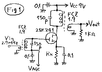
Making an Amplifier:
We know the many types of amplifier with AGC control. They say that the
forward AGC with the special designed transistor
for the forward AGC system achieves the best character. But I feel that the most famous of them is the FET gate bias control
type like as Figure1. In this circuit the gate bias is controlled by Vagc on the
figure. I can easy understand this circuit because it works same as the old vacuum
tube amplifier circuit made with 6BD6. In this experiment I used the FCZ1.9 type
coil, because I have much of them. With this coil and 150pF capacitor this circuit
works with 2.7MHz. AM modulated signal is input on the Vin terminal on the figure
from the signal generator. Different from the Vcc power, 1.5V battery and 1kohm
variable resister are used to put the minus voltage from 0 to -1.4 volts. Yes such
a bias voltage souse was called as C power in the ancient time.
図1
I made this circuit with 1k ohm for it’s source resister (Rs). But the
gain of it cannot be controlled smoothly with the change of control voltage,
Vagc. I changed Rs to 3.3k ohm. The gain of this amplifier reduced but
the controllability was better. I input the proper signal from the signal
generator and measured the output voltage with oscilloscope while I changed
the control voltage Vagc. The results are indicated on the table1 and the
black circular dot on the figure2.
table-1
| Vagc(v) | Vin(mVp-p) | Vout(mVp-p) | A=gain | gain(dB=20*logA) |
| 0 | 32 | 410 | 12.8 | 22.1 |
| -0.2 | 32 | 340 | 10.6 | 20.5 |
| -0.4 | 32 | 270 | 8.4 | 18.5 |
| -0.6 | 32 | 200 | 6.25 | 15.9 |
| -0.8 | 32 | 120 | 3.75 | 11.5 |
| -1.0 | 32 | 30 | 0.94 | -0.6 |
| -1.2 | 330 | 280 | 0.85 | -1.4 |
| -1.4 | 330 | 55 | 0.166 | -15.6 |
Figure-2
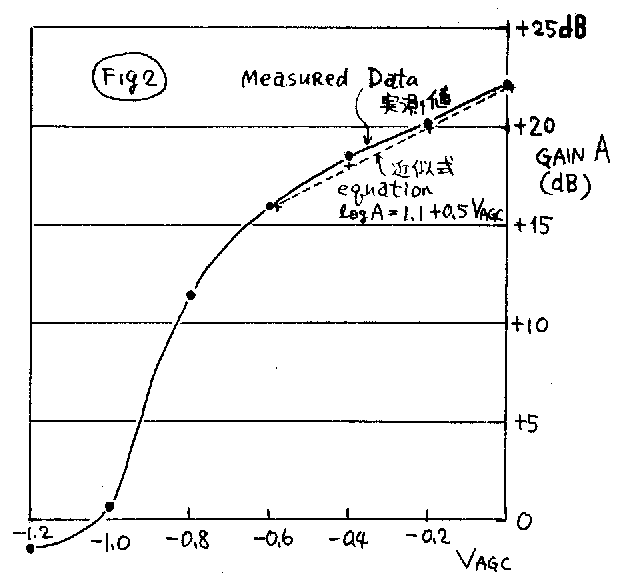
The FET transistor which I used here, 2SK241 is not a special transistor
designed to be used for gain control. The character of it is called as
the sharp cut off. So when the bias become over -0.6 volts, the gain of
this amplifier becomes quickly down. But while the Vagc is 0 to -0.6 volts,
the gain of it is controlled smoothly. Let us equalize the relation between
the Vagc and the gain, A. The vertical arc of the Figure 2, A are log scale.
And the horizontal scale of it, Vagc is linear. So I shall equalize the
relation like follows.
logA=a+bVagc……………….(1)
And from the table-1.
When Vagc=0V,tehn A=12.8
When Vagc=-0.6V,then A=6.25
INput these data for the equation(1), I get these two equations.
log12.8=a+b*0……………..(2)
log6.25=a+b*(-0.6)…………(3)
from(2) log12.8=a
So,a=log12.8=1.1
Inputting this to (3),
log6.25=1.1+b* (-0.6)
0.80=1.1+b* (-0.6)
b=0.5
I get the number,a=1.1,b=0.5
Therefore the AGCcharactor is equalized as,
logA=1.1+0.5Vagc………..(4)
In this equation the A is defined as,
A=(Vsigout/Vsigin)……….(5)
To make it sure to be equalised properly, the relation of Vagc and A is protted as dotted line on the figure 2.
CASE1: Experiment of single stage AGC
I attached the diode detector for the last amplifire. AGC cintrol voltage was got on the
point(Q) as the minus peak voltage of the out of the amplifire, point (P).
Fig3
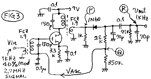
The modulation factor of the signal of my signal generator is 40%. Even
if the modulation factor was 100% the voltage of modulated signal is half
of the carrier wave. So the modulated signal is 20% of the carrier. This
diode detector is very simple and it’s efficiency is about 50%. Totally
the audio signal, 1kHz on the R point of figure 3 is only 10% of the signal
on the (P) point as measured. I inputted the proper signal on Vin point
of the figure 3. I measured the audio signal after detector on the R point
of the figure 3. The result was the table 2 and it is plotted on “Single
AGC Measured: CASE1” of the fgure5.
Table2
| Vim(mVp-p) | Vout(mVp-p) |
| 160 | 80 |
| 100 | 75 |
| 80 | 60 |
| 40 | 45 |
| 10 | 10 |
| 3.3 | 2 |
Figure5
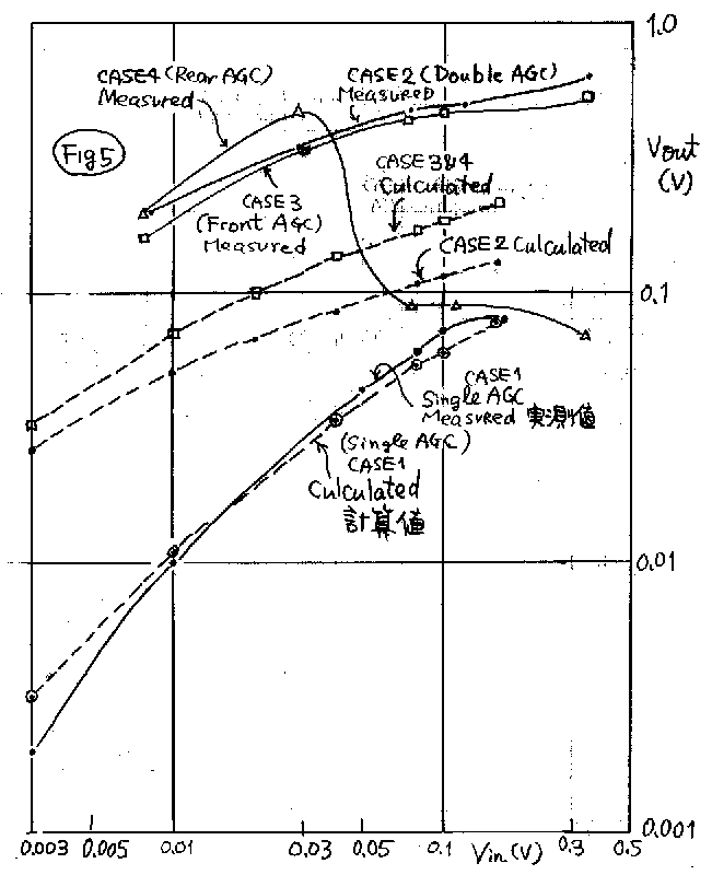
When the input signal changed from10mVp-p to 100mVp-p, the output signal changes from 10mVp-p to 75mVp-p. Here this circuit do not achive so good compression (regulation) ratio. Here the amplifier works almost as linear amplifier. My signal generator can not provide bigger signal. To know the character when it receives bigger signal, I must add the amplifier before this circuit. I will do later in this page. But in practical case, the IF amplifier usually receives these level of signals. The case of bigger input signal are not practical.
Resolution-1: With single stage amplifier the AGC can not get enough voltage
to control the gain. Single stage IF amplifier with AGC has poor regulating
character.
Calculation of regulating charactor:
I will calculate these regulating charactor as follows.
The gain of this amplifier is simulated with the last (4) equation. In
this case gain is the voltage of signal on (P) devided by input signal
Vin . Therefore,,,l
log(Vr/Vin)=1.1+0.5Vagc............................(100)
By observing the signal on (P) point and on (Q) point at the same time by osccilloscope, the voltage of (Q) point(Vagc) is known as almost same with minus peak voltage of the signal of (P) point(Vr)
Vagc=-Vr.......................................(101)
By the way, the audio signal on (R) point(Vout) is far small than the signal on (P) point(Vr). Very sorry "(P) point signal is called as Vr" may makes you confusion.
Vout=0.1V...............................(102)
(102)is changed to,
Vr=10Vout..........................(103)
input(103)to(100),,
log(10*Vout/Vin)=1.1+0.5Vagc.....................(104)
input(103)to(101),,
Vagc=-10Vout.......................(105)
input(105)to(104),,
log(10*Vout/Vin)=1.1-5*Vout......................(106)
In order to solve this equation, in order to deal more easy, let us stay Vout=y and Vin=x.
Log(10*y/x)=1.1-5y.................................(107)
10y/x=10^(1.1-5y)
10y=10^1.1*X*10^(-5y)
10y=12.5*x*10^(-5y)
y=1.25*x*10^(-5y).................(108)
I could not solve this equation. I could not
change this equation for the shape as y=f(x). I was annoyed (enjoyed) with this
equation. But I solved it at last. I used the calculation of EXEL. I stayed x, y,(1.25*x*10^(-5y)
on the EXEL sheet. I stay X as 0.01. And until the (1.25*x*10^(-5y) becomes same
or near equal as y, I changed the y for 100 times. The following table3 are the
relation between x and y as the result of this EXEL calculation. And it is plotted
on dotted line on the figure5 marked for (Single AGC: CASE1: Calculated). Yes. It
simulate the experimental data very well.
Table3
| x=Vin(mVp-p) | y=Vout(mVp-p) |
| 300 | 108 |
| 160 | 80 |
| 100 | 61 |
| 60 | 54 |
| 40 | 34 |
| 10 | 11 |
| 3.3 | 3.9 |
CASE2: Experiment and calculation of 2 Stage AGC
Next, I made the two stage amplifier with the same circuit as figure1 and detector was same as figure3. I connected the controlling voltage to two amplifiers. Please see the figure4.
Table4 is the result of the experiment. And it is plotted on figure5 as circle line named as (CASE2: Double AGC: Measured).
In this case, when the input signal has changed
from 10mVp-p to 100mVp-p, the output signal has changed from220mV to 500mVp-p. Ten
times change of input has regulated to 2.3 times change of output. Yes, far better
regulation then single one.
Resolution 2: Two stage AGC has very good character
of regulation.
Fig4
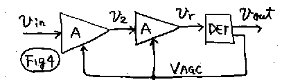
table-4
| x=Vin(mVp-p) | y=Vout(mVp-p) |
| 340 | 640 |
| 120 | 500 |
| 76 | 480 |
| 28 | 350 |
| 7.7 | 160 |
I will calculate this circuit asfollows.
I define the gain of first amplifier as A1.
A1 is altitude of output signal of first amplifire(V2) devided by input
signal(Vin). Therefore,,
A1=(V2/Vin).......................(201)
The gain of AGC amplifire is simulated wuth (4) equation. So,,
logA1=1.1+0.5Vagc.......................(202)
input(201) to (202)
log(V2/Vin)=1.1+0.5Vagc.......................(203)
from this equation,
(V2/Vin)=10^(1.1+0.5Vagc).......................(204)
By the way, same as first amplifire, the gain of second amplifiere (A2) are also indicated as,
log(Vr/V2)=1.1+0.5Vagc.......................(205)
(Vr/V2)=10^(1.1+0.5Vagc).......................(206)
By multiplying each side of (204) by (206), I can delete V2.
Vr/Vin=10^(1.1+0.5Vagc)* 10^(1.1+0.5Vagc)
=10^(2.2+Vagc).......................(207)
By the way, the work of the detector was same with last case1, I can use (101) and (105) figure in this case.
Vagc=-Vr.......................(101)
Vagc=-10Vout.......................(105)
Inputting (101) to (207), I delate Vr as,
-Vagc/Vin=10^(2.2+Vagc).......................(208)
Inputting (105) to (208), I delate Vagc as,
10Vout/Vin=10^(2.2-10Vout).......................(209)
Also in this case, for easy to deal, setting Vout=y and Vin=x,
10y/x=10^(2.2-10y)
10y=(10^2.2)*x*(10^-10y)=158x*(10^-10y)
y=15.8x*(10^-10y).......................(210)
Also in this case I solved this equation with
EXEL sheet. The got relation between x and y are indicated in the table5 and it
is plotted on figure5 as (Case2 calculated). The level is different from the experimented
data. But shape of the curve is very similar.
Table-5
| X=Vin(mVp-p) | Y=Vout(mVp-p) |
| 160 | 129 |
| 100 | 114 |
| 80 | 107 |
| 40 | 85 |
| 20 | 67 |
| 10 | 50 |
| 3 | 26 |
CASE3: Only first stage AGC of 2 stage AMP
What I do here is the main theme of this page. I had known that the two stage double AGC has a god regulating character in my experience. But I wanted to know it is how differ from only younger stage AGC. In this case the control voltage of the second stage amplifier is connected to ground and bias of the second stage is fixed with zero bias. The measured data is indicated in the table6 and it is plotted on the figure5 as (CASE3: Front AGC: Measured). I expected the regulation character of this case may be better than single case but worth than double case. But, against my expectation, the regulating character of this case was very similar with the double AGC case. I can not believe it easy. So let us make calculation.
figure6
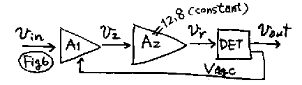
Table6
| x=Vin(mVp-p) | y=Vout(mVp-p) |
| 340 | 540 |
| 120 | 480 |
| 76 | 440 |
| 28 | 350 |
| 7.7 | 200 |
Also in this case, the gain of the first amplifire is indicated as A1
A1=(V2/Vin).............................(301)
A1 is simulated with the equation(4). So,
logA1=1.1+0.5Vagc............................(302)
input(201) to (202),
log(V2/Vin)=1.1+0.5Vagc............................(303)
from upper figure,
(V2/Vin)=10^(1.1+0.5Vagc)............................(304)
By the way, the gain of the the second amplifier is constant. so,
Vr/V2=12.8............................(305)
multiplying with each side of (304)and (305), and delate V2
Vr/Vin=10^(1.1+0.5Vagc)*12.8............................(306)
By the way, detector was same with current cas. So,
Vagc=-Vr............................(101)
Vagc=-10Vout............................(105)
inputting (101) to (306) and delate Vr,
-Vagc/Vin=10^(1.1+0.5Vagc)*12.8............................(307)
inputting (105) to (307) and delate Vagc
10Vout/Vin=10^(1.1-5Vout)*12.8............................(308)
Also in this case for easy to deal, Vout=y and Vin=x.
10y/x=10^(1.1-5y)*12.8
y=15.8*x*10^(-5y) ............................(309)
The result of the calculation with EXEL sheet is shown on table7 and it is plotted on the figure5 as CASE 3(&4) culculated. Also with the result of calculation the charactor of front only AGC was similor with that of double AGC.
table7
| x=Vin(mVp-p) | y=Vout(mVp-p) |
| 0.16 | 0.214 |
| 0.1 | 0.186 |
| 0.08 | 0.173 |
| 0.04 | 0.134 |
| 0.02 | 0.100 |
| 0.01 | 0.070 |
| 0.003 | 0.032 |
Resolution 3: The character of the front only AGC is similar with that of Double AGC. AGC is enough with only youngest stage.
CASE4: Rear only AGC
As a last case of this experiment I measured the case of the AGC was activated only the rear stage of the double amplifier. In this case the front amplifier works as linear amplifier with the gain of 12,8. The result of experiment is shown on the table8 and it is plotted on the figure5 as(Case4: rear AGC: Measured). The result was very bad. When the input signal be over 30mV, the second amplifier come into the over driven. The shape of the wave on the cathode of the detector was crushed. So the output signal become smaller than low level input.
Figure7
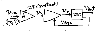
Table-8
| X=Vin(mVp-p) | y=Vout(mVp-p) |
| 340 | 70 |
| 120 | 90 |
| 76 | 90 |
| 28 | 480 |
| 7.7 | 200 |
The result of the culculation will indicate the measured data? I will do
that.
The first stage of the amplifire is constand gain. so,
V2/Vin=12.8.......................(401)
The sesond stage gain is stated as A2.
A2=(Vr/V2)...................(402)
The second stage is AGC amplifire so it is equated with (4).
logA2=1.1+0.5Vagc......................(403)
put(402)to(403)
log(Vr/V2)=1.1+0.5Vagc.......................(404)
from this figure
(Vr/V2)=10^(1.1+0.5Vagc).................(405)
multiple(402)with(405) and delateV2. So.
Vr/Vin=10^(1.1+0.5Vagc)*12.8.....................(406)
This equation (406) is same with (306). Therefore the character of rear only AGC must be same with that of front only AGC. Please see the figure5. Until the input signal are lower than 30mVp-p, CASE3 and 4 indicated the similar character.
By the way, Figure7 is same with figure3 with bigger signal generator including amplifier. Therefore CASE 4 (Rear only AGC) shows the character with 12.8 times bigger input signal of CASE 1 ( Single AGC).
Resolution 4: When the AGC was activated only
the last stage of the IF amplifier, the range of good regulation be narrow. With
small signal it do not regulate. With big signal it has distortion. To get a good
regulation the total gain of the arranged amplifier should have the enough gain
to waste. AGC should be activated as front stage as possible.
Another remaining two issues about the Auto gain control:
1. When I made a vacuum tube radio receiver, I measured about 0.1 volt AGC voltage even without connecting the antenna for it. This AGC voltage may be born from the conversion noise of 6BE6. So the gain of the radio was waste without any purpose. Conversion noise should be considered to make good AGC controlled radio.
2. In order to hear 9MHz band Voice of America (VOA) with narrow crystal filter, I made also FET transistor receiver. VOA signal had the phasing with the period of 1Hz. Originally I used the AGC with timing factor of 1second. The audio signal are masked when the radio signal becomes weaker. I understood that was caused by the delay of the AGC system. I defined this phenomena as “AGC delay masking”. I changed the time factor of the AGC to 0.1second. It worked well. You can adjust the time factor only change the capacitor of AGC line with the experience of your test usage. The adjustment of this factor are not so critical.
back to index
**************************Japanese Language*******************************************
AGCの研究
AGCの研究
はじめに:我々がトランシーバーや受信機を作る際に、AGC(Auto Gain Control)すなわち自動音量調節機能を採用することがままあります。これには下記のごとき作用があります。
① AGCなしでトランシーバーを作った場合、ちょうど交信しやすい距離の相手と交信しているうちはいいのだが、それよりも近くに交信相手がくると、音が割れてしまい、聞きにくい。AVCがあれば、近くでも問題なく交信ができる。
② 同様に、中波のラジオにおいても、遠くの放送局(本来は弱い信号)から近くの放送局(強い信号)に選局ダイアルを回したときに、いちいち音量調節ダイアルを回さずとも、同じ強さの音量で聞くことができる。
③ 短波の、ラジオを作る際に、隣の国(日本では韓国や中国)の放送は聴きやすいのだが、遠くの国(日本からは、たとえばアンデスの声放送やラジオウクライナなど)の放送を聴く際には、フェージング現象といって、音量が1秒から5秒くらいのサイクルで大きくなったり、小さくなったりする現象が発生して、大変に聞きにくい。AGCがあれば、このフェージング現象を緩和してくれるので、聞きやすくなる。
私は、いままで、トランシーバーや受信機を作る際に、雑誌などのAGC回路をまねして、そのまま採用し、それでちゃんと効果がえられたので、それでよしとしてきましたが、今回久しぶりに「高1中1」の受信機を真空管で作る際、AGCの調整電圧を中間周波増幅器(6BD6)にかけるか、高周波増幅(6BA6)にかけるか、はたまた周波数変換(6BE6)にかけるかで、なやんだので、この際原理的に研究してみることにしました。実験は、真空管では電圧が高くてあぶないので、下記のごとくFETを使ってやりました。
増幅器の作成と特性の把握:
AGCをかける増幅器はいろいろあります。フォワードAGCの研究を先輩の山村さんは以前CQ誌に発表されていました。しかし、現在なんといっても一番一般的なのは、図1のような、FETのゲートバイアスを調節するタイプでしょう。この方式は、FETの入力インピーダンスが高いので、AGC電圧も高いインピーダンスすなわち低電力で駆動できるというメリットがありますし、なんといっても真空管からのAGC回路と同じ考え方でいいというところが私のような親父には向いています。周波数は何でもよいのですが、455kHzの中間周波トランスが多数手持ちになかったので、FCZ1.9を使い、周波数は2.7MHzの信号をシグナルジェネレーターから入れています。その入出力の信号の強度をオシロスコープで計測しています。電池とボリュームでマイナス電源(昔風にいうところのC電源)を作って、これをVagcに印加しています。
図1
はじめは、この回路で、ソースの抵抗Rsは1kオームでしたが、AGC電圧の変化に対して、スムーズに利得が変わらなかったので、Rsは3.3kオームとしました。こうして、Vagcを0ボルトから-1.4ボルトまで変化させたときの、利得Aの変化を計測したのが表1で、これをプロットしたのが、図2です。
表1
| Vagc(v) | Vin(mVp-p) | Vout(mVp-p) | A=gain | gain(dB=20*logA) |
| 0 | 32 | 410 | 12.8 | 22.1 |
| -0.2 | 32 | 340 | 10.6 | 20.5 |
| -0.4 | 32 | 270 | 8.4 | 18.5 |
| -0.6 | 32 | 200 | 6.25 | 15.9 |
| -0.8 | 32 | 120 | 3.75 | 11.5 |
| -1.0 | 32 | 30 | 0.94 | -0.6 |
| -1.2 | 330 | 280 | 0.85 | -1.4 |
| -1.4 | 330 | 55 | 0.166 | -15.6 |
図2
ここで使用した2SK241は、AGC用に考慮された特性を持っているわけではないので、バイアスが深くなると、急にゲインがなくなってしまいます(いわゆるシャープカットオフ特性)。しかし、それでも、バイアスが0からー0.6までは、かなりスムーズに利得が調節できています。この間のバイアス電圧VagcとゲインAの関係を数式化しましょう。縦軸Aは対数軸で、横軸Vagcはリニアスケールです。その関係は右上がりの直線ですから、
logA=a+bVagc……………….(1)
と置くことができます。ここで、
Vagc=0V のとき A=12.8
Vagc=-0.6V のとき A=6.25 という実験データを(1)式に代入して、
log12.8=a+b*0……………..(2)
log6.25=a+b*(-0.6)…………(3)
(2)式から、
log12.8=a
よって、a=log12.8=1.1
これを(3)に代入して、
log6.25=1.1+b* (-0.6)
0.80=1.1+b* (-0.6)
b=0.5
こうして、(2)と(3)式を解くとa=1.1,b=0.5ともとまるので、図1の増幅器のAGC電圧特性として、
logA=1.1+0.5Vagc………..(4)
が求まりました。ただし、ここで、
A=(Vsigout/Vsigin)……….(5)
これを確認のために図2の点線で近似式特性としてプロットしてあります。
1段AGCの実験と計算:CASE1
図1の増幅器にダイオード検波器を追加して、AGC電圧と低周波信号を別々にとりだせるようにしたのが、この図3の回路です。
図3
この図の入力にシグナルジェネレーターからの振幅変調信号を入力すると、(P)点に増幅された信号が出てきます。これをダイオードで検波するのですが、その際、ダイオードがカソード(図のK)を入力側にして取り付けられているので、出てくる信号はマイナスになります。図の(Q)点には(P)点の高周波信号の尖頭値の値がほぼマイナスの直流電圧となって現れます。一方、検波された信号のなかの低周波(ここでは1kHz)信号はコンデンサーを通って(R)点に現れますが、私のシグナルジェネレータのAM信号は変調率が40%です。もともと変調率が100%でも、低周波の振幅は、搬送波の50%なのですから、変調率が40%では、その半分以下で、さらに(R)点において信号の一部が減衰しているので、実測上(R)点に現れる低周波信号は、(R)点の信号の約10%にすぎません。図3の入力に入れた信号Vinと、出力された低周波信号Voutの関係を入力レベルを変えて実測したのが、表2です。これをプロットしたのが、図5の下側の(CASE1SingleAGC-Measured実測値)と書いてある実線です。
表2
| Vim(mVp-p) | Vout(mVp-p) |
| 160 | 80 |
| 100 | 75 |
| 80 | 60 |
| 40 | 45 |
| 10 | 10 |
| 3.3 | 2 |
図5
入力レベルが10mVp-pから100mVp-pへ、10倍に大きくなったときに、出力レベルは10mVp-pから75mVp-pへと7.5倍になっているので、すこしだけ圧縮されていますが、たいしたことはありません。この間はまだほとんどリニアーな増幅です。それよりもさらに入力が大きくなって、160mvになったときに、入力信号は1.6倍にたいして、出力信号は75mVp-pから80mVp-pまでしか増加していないので、ここでやっとAGCが働き始めていることがわかります。私のシグナルジェネレータではこれだけしか入力レベルが上げられないので、これ以上のレベルの実測はこの回路の前段に増幅器をつけて行う必要がありますが、それは後でやることにします。それに、この後どうなるかは気にかかるところではありますが、実際の受信機の中間周波増幅の後段は、このレベルで働くことがおおいので、これ以上大きなレベルがどうなっているかは、実用上は役にたたない部分であるともいえます。
結論①:中間周波1段の増幅器にAGCをかけても、よっぽど大きな入力の信号だけが抑えられるという効果は得られるものの、通常は十分なAGCがかかる前のレベルでしか、動作できないので、結果としてAGCがかからず、よいAGC特性は得られない。
この場合のAGC特性の計算:
以上の実験の回路のAGC特性を計算で検証してみます。
図3における、入力信号Vinと(R)点信号Vrの関係は、(4)式から、
log(Vr/Vin)=1.1+0.5Vagc…………………….(100)
ここで、検波器のAGC電圧は、実測上(R)点電圧のマイナス値そのものとして扱って差し支えないので、
Vagc=-Vr…………………………(101)
一方、検波器の出力である、低周波信号はさきほど説明したように、高周波信号の振幅の10%しか実測上ないので、Voutをここでは低周波信号の出力レベルと定義すると、
Vout=0.1Vr…………………….(102)
の式で表せます。
(102)より、Vr=10Vout………………..(103)
(103)を(100)に代入して、
log(10*Vout/Vin)=1.1+0.5Vagc…………(104)
(103)を(101)に代入して、
Vagc=-10Vout…………………..(105)
(105)を(104)に代入して、
log(10*Vout/Vin)=1.1-5*Vout…………(106)
この式を解くために、簡単のために記号を簡略化するため、Vout=y,Vin=xと置き換えて、
Log(10*y/x)=1.1-5y…………………(107)
10y/x=10^(1.1-5y)
10y=10^1.1*X*10^(-5y)
10y=12.5*x*10^(-5y)
y=1.25*x*10^(-5y)……………..(108)
この式は、私の数学力ではy=f(x)の形に、変形できない。さてここで、3日ほどなやんだあげく、この式をエクセルで計算させるようにエクセルをくんで、たとえばX=0.01と置いた時の1.25*x*10^(-5y)の値をいろいろなYに対して計算させて、それがy自体とほぼ(3桁まで)等しくなったときのyを求める。このようにして、(108)式のxとyの関係をいろいろなxの値に対してもとめた表が、下の表3で、これをグラフにしたのが図4の点線です。ここでは、計算値と実測値がよくあっていますが、計算値といっても、あっちこっちで、実験の結果を使って作った式ですから、あうのは当たり前です。ここまでは、式を使って何かを証明しようというわけではなく、式を作っている段階です。
表3
| x=Vin(mVp-p) | y=Vout(mVp-p) |
| 300 | 108 |
| 160 | 80 |
| 100 | 61 |
| 60 | 54 |
| 40 | 34 |
| 10 | 11 |
| 3.3 | 3.9 |
2段同時AGC回路の実験と計算:CASE2
次に、いわゆる中2、中間周波2段増幅の場合を実験してみます。図3における、増幅器を2つ直列に並べて、2段増幅し、これの両方にAGC電圧を印加します。
図4
このときの入力信号Vinと出力低周波信号Voutの関係を実測したのが、表4で、これをプロットしたのが、図5の上のほうにある丸実線(Measured Siganl:Case2実測値)です。
表4
| x=Vin(mVp-p) | y=Vout(mVp-p) |
| 340 | 640 |
| 120 | 500 |
| 76 | 480 |
| 28 | 350 |
| 7.7 | 160 |
入力信号が0.01Vp-pから0.1Vp-pへと10倍増加した際に、出力信号は0.22Vから0.5Vへと2.3倍にしか増加しておらす、そうとう平均化されていることがわかります。ちなみに、ここでは、入力が0.01Vp-pとか0.1Vp-pのときの値は、直接実験した値ではなく、実験した値をグラフで補間した値です。
結論2:2段同時AGC回路は1段AGCに対して、AGC特性が大幅に改善される。
さて、以上の実験の回路のAGC特性を計算で検証してみます。
まず、1段目の利得A1を考えると、
A1=(V2/Vin)………………….(201)
ここで、1段目は利得制御増幅器で、その特性は(4)式により、下記に表せる。
logA1=1.1+0.5Vagc………..(202)
(201)を(202)に代入して
log(V2/Vin)=1.1+0.5Vagc………..(203)
この式から、
(V2/Vin)=10^(1.1+0.5Vagc)………..(204)
一方、2段目の増幅器の利得も同様に、下記のごとく表せる。
log(Vr/V2)=1.1+0.5Vagc………..(205)
この式からも同様に変形して、
(Vr/V2)=10^(1.1+0.5Vagc)………..(206)
(204)と(206)式を掛け合わせて、中間利得V2を消去すると、
Vr/Vin=10^(1.1+0.5Vagc)* 10^(1.1+0.5Vagc)
=10^(2.2+Vagc)………………(207)
いっぽう、検波器の働きは先ほどの場合と変わらないから、
Vagc=-Vr…………………………(101)
Vagc=-10Vout…………………..(105)
の2式は今回もそのまま。
(101)式を (207)式に代入してVrを消去すると、
-Vagc/Vin=10^(2.2+Vagc)………………(208)
さらに、(105)式を (208)式に代入してVagcを消去すると、
10Vout/Vin=10^(2.2-10Vout)………………(209)
今回も、この式を解くために、簡単のために記号を簡略化するため、Vout=y,Vin=xと置き換えて、
10y/x=10^(2.2-10y)
10y=(10^2.2)*x*(10^-10y)=158x*(10^-10y)
y=15.8x*(10^-10y)…………….(210)
この式を、さきほどと、同様にエクセルを1000回たたいて手で漸近させて解いたのが、下記の表5であり、それをプロットしたのが、上の表5の(210)式=丸点線です。出力の絶対値はだいぶずれていますが、AGCの係り具合に関しては、実験結果とよく似たカーブになっています。
表5
| X=Vin(mVp-p) | Y=Vout(mVp-p) |
| 160 | 129 |
| 100 | 114 |
| 80 | 107 |
| 40 | 85 |
| 20 | 67 |
| 10 | 50 |
| 3 | 26 |
2段増幅器の前段のみAGCをかけた回路の実験と計算:CASE3
次に、中間周波2段増幅の前段のみAGCをかけた場合を実験してみます。図4における、増幅器を2つ直列に並べて、2段増幅し、これの前段のみにAGC電圧を印加します。後段は、AGCラインをアースにつないで、ゼロバイアス固定とします。実を言うと、今回本当にやりたかったのはこの実験です。多段AGCがよい結果になることは経験的にもわかっていましたが、前段AGCと多段AGCの比較をしたかったのです。図6の回路となります。
図6
このときの入力信号Vinと出力低周波信号Voutの関係を実測したのが、表6で、これをプロットしたのが、図5の四角実線(Case3:FrontAGC:Measured)です。
表6
| x=Vin(mVp-p) | y=Vout(mVp-p) |
| 340 | 540 |
| 120 | 480 |
| 76 | 440 |
| 28 | 350 |
| 7.7 | 200 |
予想としては、両段にAGCをかけたときほどはよくはないと想像していましたが、あにはからんや。測定の結果は、さきほどの2段同時AGC回路の結果とほとんど同じでした。ちょっと信じられないので、計算でも同様になるかどうか、検討してみます。
まず、1段目の利得A1を考えると、
A1=(V2/Vin)………………….(301)
ここで、1段目は利得制御増幅器で、その特性は(4)式により、下記に表せる。
logA1=1.1+0.5Vagc………..(302)
(201)を(202)に代入して
log(V2/Vin)=1.1+0.5Vagc………..(303)
この式から、
(V2/Vin)=10^(1.1+0.5Vagc)………..(304)
一方、2段目の増幅器は固定なので、下記のごとく定数である。
Vr/V2=12.8………..(305)
(304)と(305)式を掛け合わせて、中間利得V2を消去すると、
Vr/Vin=10^(1.1+0.5Vagc)*12.8………………(306)
いっぽう、検波器の働きは先ほどの場合と変わらないから、
Vagc=-Vr…………………………(101)
Vagc=-10Vout…………………..(105)
の2式は今回もそのまま。
(101)式を(306)しきに代入してVrを消去すると、
-Vagc/Vin=10^(1.1+0.5Vagc)*12.8………………(307)
(105)式を(307)しきに代入してVagcを消去すると、
10Vout/Vin=10^(1.1-5Vout)*12.8………………(308)
今回も、この式を解くために、簡単のために記号を簡略化するため、Vout=y,Vin=xと置き換えて、
10y/x=10^(1.1-5y)*12.8
y=15.8*x*10^(-5y) ………………(309)
この式を、さきほどと、同様にエクセルを1000回たたいて手で漸近させて解いたのが、下記の表7であり、それをプロットしたのが、上の表5の(309)式=四角点線です。出力の絶対値は実測値とだいぶずれていますが、AGCの係り具合に関しては、実験結果とよく似たカーブになっています。とにかく、理論的に計算した、両AGCと前段AGCがあまり変わらないカーブになるのは本とらしいことがわかります。
表 7
| x=Vin(mVp-p) | y=Vout(mVp-p) |
| 0.16 | 0.214 |
| 0.1 | 0.186 |
| 0.08 | 0.173 |
| 0.04 | 0.134 |
| 0.02 | 0.100 |
| 0.01 | 0.070 |
| 0.003 | 0.032 |
結論3:2段同時AGC回路にたいして、その前段だけにAGCをかけたものは、総合特性が2段同時AGC回路と実用域においてほとんど変わらない。AGCは最前段にだけかければ十分であると換言できる。
2段増幅器の後段のみAGCをかけた回路の実験と計算:CASE4
最後に、中間周波2段増幅の後段のみAGCをかけた場合を実験してみます。図7のごとく、後段のみにAGC電圧を印加します。前段は、AGCラインをアースにつないで、ゼロバイアス固定とします。
図7
このときの入力信号Vinと出力低周波信号Voutの関係を実測したのが、表8で、これをプロットしたのが、図5の三角実線(Case4:RearAGC:Measured)です。
表8
| X=Vin(mVp-p) | y=Vout(mVp-p) |
| 340 | 70 |
| 120 | 90 |
| 76 | 90 |
| 28 | 480 |
| 7.7 | 200 |
予想としては、前段にAGCをかけたときほどはよくはないと想像していましたが、そのとおりでした。途中から、信号がひずんでしまい、かつ入力信号が大きいほど、出力信号が小さくなるという逆転現象が発生しています。これは、2段目のアンプが動作領域いっぱいで増幅できる領域を超えた入力を受け、波形の頭がつぶれてしまい、このため、振幅変調された波形の頭がつぶれたために、結果として波形の変調が浅くなったとオシロスコープで観察されました。
まず、1段目の利得A1を考えると、増幅器は固定なので、下記のごとく定数である。
V2/Vin=12.8………..(401)
次に2段目の利得A2は、下記のごとく表せる。
A2=(Vr/V2)………………….(402)
ここで、2段目は利得制御増幅器で、その特性は(4)式により、下記に表せる。
logA2=1.1+0.5Vagc………..(403)
(402)を(403)に代入して
log(Vr/V2)=1.1+0.5Vagc………..(404)
この式から、
(Vr/V2)=10^(1.1+0.5Vagc)………..(405)
(402)と(405)式を掛け合わせて、中間利得V2を消去すると、
Vr/Vin=10^(1.1+0.5Vagc)*12.8………………(406)
この(406)式は(306)しきと同じ式だから、結果として、後段のみAGC(Case4)は前段のみAGC(Case3)と同じ特性に計算上はなるはずである。実際図5をみれば、信号が飽和するまでは、後段のみAGCは前段のみAGCと近い特性を示していました。
尚、話がもどりますが、1段増幅AGCの前に直線増幅器を置いた場合が図7ですから、図7の回路の特性、すなわち図5の三角実線は、図4の実線の12.8倍先(右側)の特性を示していることになります。すなわち、1段AGCでも大きな入力信号のレベル(この場合、入力信号で0.1から0.5Vp-p)の範囲なら良好なAGC特性が得られることがわかります。
結論4:中間周波最終段だけにAGCをかけると、かなり大きな入力になるまでAGCがかからず、またある程度以上の入力になると今度は増幅器が飽和してしまうので、結果的に、うまくAGCがかかる範囲(ダイナミックレンジ)が狭く、良いAGC特性が得られない。AGCはできるだけ、前段にかけるのがよい。
最後に二つの話題:
1.真空管ラジオを作っていて気が付いたのですが、何も放送信号を受けていない、それどころか、アンテナをつながない時でも、ある0.1ボルト程度のAGC電圧が発生しており、このため中間周波の利得が落っこちています。6BE6のコンバーターで発生するノイズでAGCがかかっているようで残念でなりません。
2.FET(2SK241)を2段つかった短波ラジオを製作してみました。9MHz帯のVOA(Voice of America)を聞いていたところ、1秒ほどの周期のフェージングで聞こえてきます。これを時定数1秒のAGCでうけると、AGC電圧の変動が入力信号の変動よりも遅れるために、信号の弱くなってゆくときに信号がマスキングされる現象が発生します。これを、AGC遅れマスキングと命名しました。AGCの時定数は0.1秒程度が良いようです。これは、AGC回路にいれるコンデンサーで間単に調節できるので、放送をききながら、調節するのがよいです。