A- class double ended push , push audio amplifier
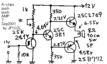
*** Pleas look the schematic. This amplifier do not have any capacitor. And all the stage is connected directly. I will indicate you the all over character of this gear first.
*** power voltage 12V
*** power current 0.25A
*** power source 3W
*** maximum output power 250mW
*** voltage gain 21dB
*** input impedance 10kohm*
** frequency character if flat from 50Hz to 50kHz (flat means less than 0.5dB, lower than 50Hz and higher than 50kHz cannot be measured with my instruments)
*** output noise cannot be measured (less than 1mV)
*** Work of each stage
***** 1. The first stage is source grounded zero bias amplifier. Generally speaking, the FET can deal not only minus input on the gate but also plus input voltage on it*s gate. Especially, Y class 2SK241 (2SK241Y) is classified as small Idss (zero bias drain current) but it has wide range for it*s plus side. The voltage drop of the resister on the drain of the 2SK241 is decided by the Idss, we must tune the voltage drop by tuning the potentiometer. Please tune it the static voltage of drain of 2SK241 to be about 4.5V.
***2. Next stage 2SC381 is the signal divider. The static voltage of 2SC381 is minus 0.5V from it's base. And the phase of the signal on the emitter of the 2SC381 is the same with the base of the 2SC381 (0drgree). On the other hand, On the collector of 2SC381 is connected the same resister with the emitter of 2SC381. And the current of collector of 2SC381 is almost the same with the current of emitter of 2SC381. Therefore the voltage drop of the resister on the collector of 2SC381 is the same with the voltage drop of the resistor of the emitter of 2SC381. Therefore the static voltage of the collector of 2SC381 becomes 12 Volt minus 3.87 volts, equal 8.13volt. real voltage became 7.21 volts. I think the difference is because of the difference of the resistor. On the collector of the 2SC381 comes the inverted signal from the base of 2SC381 (180 degree).
***3. Next stage of 2SC2749 is only the emitter follower. The voltage of the emitter of 2SC2749 becomes 0.5 volt lower than the base of the 2SC2749. The signal phase of the emitter of the 2SC2749 is the same phase from the base of the 2SC2749. Therefore the phase of the 2SC2749 is 180 degree from the base of the 2SC381.
***4. 2SB772 works also as only emitter follower. It is PNP type. Therefore the emitter of 2SB772 becomes 0.5 volt higher than the base of the 2SB772. The signal phase of emitter of 2SB772 is same with the base of the 2SB772. Therefore the phase of the emitter of 2SB772 becomes 0 degree from the base of 2SC381.
***5. 8 ohm speaker is connected between the emitter of 2SC2749 and emitter of 2SB772. The each voltage of it is decided from the voltage of collector and emitter of 2SC381. That is 6.55V and 4.58V statically. 8 ohm speaker has 8 ohm impedance and 8 ohm static resistance. Therefore the static current of the speaker is decided by the voltage (between the emitter of 2SC2749 and 2SB772, 6.55V-4.58V=1.97V ) and the static resistance of the speaker ,8 ohms. The current of the speaker becomes 1.97V/ 8 ohm = 0.25A. It becomes also the current of 2SC2759 and 2SB772. Therefore these transistor has power loss 5V*0.25A=1.25watt. Therefore these transistors should be attached on the 5W class heat sink. 2SC2749 and 2SB772 are driven by opposite phase. Therefore this circuit should be called as push , push circuit, while the normal single ended circuit are called as push pull circuit.
*** Merits: This circuit do not have any "Time factor". Therefore the frequency character of this amplifier is excellent. You must tune the voltage of the drain by tuning the potentiometer , but only the rough tuning is enough.
***Demerit: All stage of this circuit works as A class. Therefore this amplifier has low power efficiency. Power source needs 3W. And maximum output power is 250mW. Power efficiency is lower than 10%. But it is normal with A class amplifier. If you want to get more power output, you can tune the potentiometer , and make the voltage drop between the speaker be bigger. But then you needs more power source current. 250mW is enough to the radio receiver. So I introduce this circuit with this situation. Thank you.
acpp.gif
Introduction of the transistors used in this circuit
*** 2SK241: Maker = Toshiba: usage = FM, VHF: Idmax = 30mA: Pdmax= 200mW: gm= 10 mS typical: Crs= 0.035pF typical: Nf=1.7dB at100MHz: Power gain is 28dB on 100MHz
***2SC381: Maker = Toshiba: Usage = RF: Vcbo = 40V: Icmax = 20mA: Pcmax = 100mW: hfe= 25 to 140: ft= 250MHz
***2SC2749: Maker = NEC: Usage = Switching: Vcbo = 500V: Icmax = 10A: Pcmax = 100W: hfe= 35 typical: ton=1micro second
***2SB772: Maker = NEC: Usage = Power amp, Switching: Vcbo = -40V: Icmax = -3A: Pcmax = 10W: hfe= 160 typical: ft=80MHz
A級プッシュプッシュオーディオ電力増幅器
***とにかく回路図をご覧ください。まったくコンデンサーが無い全段直結の音声電力増幅器です。今回は最初に全体の性能を諸元でしめします。
***電源12V
***電源消費電流0.25A
***消費電力3W
***最大出力250mW
***電圧利得21dB
***入力インピーダンス10kオーム
***周波数特性50Hzから50KHzまで0.5dB以内
***出力ノイズ計測不能
*** 回路の動作と特徴
***1.最初のFETはゼロバイアスで軽く動作しています。FETは一般に入力電圧が0付近では、プラス入力もマイナス入力も扱えます。特に2SK241のYクラスはIdssが小さい分、プラスの入力にも対応可能です。但し、この部分は、ゼロバイアスの生のドレーン電流でドレーンの直流電位が決定されるので、個々のFETのばらつきにあわせて調整が必要です。ドレーンの直流電位が4Vから6Vまで調整できる様にドレーンの半固定抵抗を選び、大体4.5V(大体でOK)になる様に調整してください。
***2.次の2SC381は信号分割器です。エミッターの直流電位はベースの直流電位から0.5V引いた電位になります。またここの出てくる信号は初段増幅器のドレーンの信号と同じ位相(0度)です。一方、2SC381のコレクターにはエミッターと同じ抵抗が付いていて、またエミッターとほとんど同じ電流が流れるので、結果的にコレクターの抵抗の両端にはエミッター抵抗と同じ電圧降下が発生します。エミッターの電位がだいたい4Vなので、コレクターの電位は12Vからこの4Vを引いた8Vが現われます。実測値が7.21Vと少しずれているのは、抵抗の値のばらつきでしょう。またここにはベースの信号が反転して現われます。(位相180度)
***3.この2SC381のコレクターにつながっている2SC2749はただのエミッターフォロワーです。ですから、2SC2749のエミッターにはベースよりも0.5V低い電位になります。またその信号は2SC381のコレルターと同じ位相で、すなわち180度です。
***4.2SC381のエミッターにつながっている2SB772もまたただのエミッターフォロワーです。ここはPNPトランジスターなので、エミッターの電位はベースよりも0.5V高くなります。そこの位相は2SC381のエミッターと同じ0度です。
***5.2SC2749のエミッターと2SB772のエミッターの間にはスピーカーがつながります。2SC2749のエミッターの電位も2SB772のエミッターの電位も前段の電位で、一義的に決まってしまうので、2SC2749と2SB772のエミッター間の電位差をスピーカーの直流抵抗で割った値が、アイドル電流になります。ここではスピーカーの直流抵抗が8オーム、(インピーダンスも公称8オームですが、直流抵抗も実測8オームでした。)両端の電位差が6.55V−4.58V=1.97Vですので、アイドル電流は1.97V/8オーム=0.25Aです。安定化電源のアンペアメーターの振れも、ちょうど0.25Aで、計算とピッタリでした。尚、2SC2749と2SB772には常時1Wを超える電力が消費されるので、必ず5Wクラス以上のヒートシンクを付けてください。2SC2749と2SB772は交流的に逆送で運転されるので、通常のプッシュプルと異なり、プッシュプッシュ増幅器になります。
***長所:とにかくなにも時定数を持つ部品がありませんので、周波数特性はどこまでもフラットです。私の手持ちの50Hzから50kHzまでのオーディオ発振器の波形の範囲では、まったく利得はフラットでした。グラフにしてもばかばかしいので、グラフにしません。こんな周波数特性の低周波電力増幅器はちょっとこうも簡単な回路では普通作れないと思います。もちろん歪みは、オッシロでスピーカーの両端の波形を計った限りまったくありません(出力1Vp—p時)。また、本機では、すべてがA級で動作しているので、バイアスの調整は必要ですが、大体でOKです。通常のシングルエンドプッシュプル増幅器に比べると、調整は極めてラフです。ここもアマチュア向けでしょう。
***短所:なにしろA級ですから、アイドル電流を食います。電源消費電力が、12Vの0.25A、すなわち3Wなのに比べて、最大オーディオ出力電力は250mWと1/10程度です。しかしこれは、A級増幅器としては当たり前の事です。2SK241のドレインの抵抗を調整して、出力である2SC2749と2SB772のエミッター間の電位差を大きくし、アイドル電流を増やしてやると、電源電力は食いますが、最大出力電力も大きくなります。まあ、250mWという値は、個人的に聞くには十分なので、この値でご紹介してみました。
back to index