21MHz 1W SSB and CW Transceiver----21m1wph.gif
 On
these days the HF condition becomes better and better. I have waited that
for this five years from last cycle. It is 6 jun 1998 today. Therefore
I decided to lift new antenna for 21MHz in my house. Yes, It is quite big
sloping dipole hihi! And I made this new transceiver to operate CW and
SSB with one box of machine. In Japan we can get from 10.595 to 10.695
10kHz step CB-junk crystals very cheap. I got many such crystals about
five years ago with 20 yens by a piece. Therefore I used these crystals
for ladder filters and oscillators. Double harmonics of the SSB local oscillator
10.6176 * 2 = 21.2352MHz becomes on the frequency of the band. But I dodge
the frequency. Please see the frequency diagram! I live on the 100km north
of Tokyo. In my city the TV signal came from Tokyo is not so strong. Therefore
21MHz amateur signal happens interference for TV easily for the third channel
of it. I made one more linear amplifier and I could get 10W power output.
But I must give up to use it because of TVI. On this project I used 24V
relays with 20V Vcc. They was cheap. I used many 2SC1815 transistors. I
got them with 1500 yens by 200 pieces. They ware also cheap. Today I used
this transceiver. I could contact with nine Amateurs on Japan with CW and
SSB. Now I am waiting to be better condition. If it comes, I will make
long QSO with California. For example ," FINAL OF MY TRANSCEIVER IS
SMALL TRANSISTOR NAMED 2SC1815 // IT IS SIMILAR AS 2N2222 // I USE 6 TRANSISRORS
PARALLEL AND PUSHPULL // SORRY I MUST GO TO SHOPPING WITH MY FOUR GANGS
// THEREFORE I MUST SAY 73"
近頃、噂によると、だいぶ今回のサイクルも上がってきたみたいです。(1998.6.6)そこで、21MHzのSSBとCWが運用できるトランシーバーを作ってみました。ここで使ったのは、10.595や10.615MHzのCBのジャンクの水晶で、1個20円で、以前たくさん買っておいた物です。今でも、秋葉原や通信販売で入手可能です。これを、発振器や水晶フィルターの自作に使用しています。内部発振の10.615MHzの二倍の高調波が受信周波数範囲の21MHzバンドの中に入って来てしまいますが、周波数をよけて使用しています。私は,東京から100km
北の土浦市に住んでいます.私の町では,東京からのテレビの信号が弱いので、21MHzのアマチュア無線の信号はテレビの第3のチャンネルに簡単にTVI(いわゆるアイちゃん)を発生してしまいます.10Wリニアーも作って、一度は箱に入れてみたのですが、使えませんでした。送受信の切り替えには、リレーを6個使っています。24V用のリレーを20V電源で使っています。また、トランジスターには2SC1815を多用しています。200個1500円で買った物です。今日1日で国内9局とCWやSSBで、QSOしました。はやく、もっとコンディションが上がって、西海岸の局とCWの平文でだらだらとロングQSOできないかな、と待っている今日このごろです。
Frequency relation of each oscillator and transmit
In Japan ,we can use from 21.000 to 21.150 for CW. But about 90% of domestic
QSO's are made 21.13+-10kHz. Therefore this CW channel is enough for me.
On SSB channel 1,I can hear many domestic SSB signal. Here is the most
useful frequency of SSB in Japan. On SSB channel 2, I can hear some signal
from HL,YC and BV.
周波数関係に関して
日本では,CW 用周波数として21.000MHzから21.150MHzを使うことができます.しかし、およそ国内のQSOの90
パーセントが,21.13+−10kHzで行われています.それゆえに,このトランシーバーのCWチャンネルは,私には十分に思えます.SSBチャンネル1で,多くの国内のSSB
シグナルを聞くことができます.ここに21MHzでは、国内SSBの最も頻繁に使われる周波数があります.SSBチャンネル2では,HL
,YC ,およびBVからの信号を聞くことができます.
| Channel |
Xal of VXO |
f VXO max |
f VXO min |
f local |
f out max = f VXO max * 3-f local |
f out min= f VXO min * 3-f local |
| ch.CW |
10.595 |
10.5758 |
10.5875 |
10.6146 |
21.1128 |
21.1479 |
| ch.1 |
10.615 |
10.5957 |
10.6075 |
10.6176 |
21.1695 |
21.2049 |
| ch.2 |
10.645 |
10.6857 |
10.6975 |
10.6176 |
21.2595 |
21.2949 |
Block Diagram of SSB transmitter
dinamic
mic |
-> |
audio
amp |
->
IF
port |
D.B.M |
->
RF
port |
10.6176
SSB filter |
-> |
IF
amp |
-> |
single balanced
Mixer |
-> |
21MHz
B.P.F |
-> |
Driver
amp |
-> |
Final
amp |
-> |
Low pass
filter |
-> |
ANt |
|
|
|
|
To LO
port
of
DBM |
|
|
|
|
|
to emitter
of S.B.M |
|
|
|
|
|
|
|
|
|
|
10.6176
SSB
local OSC |
-> |
Buffer |
-> |
upside |
|
ch.1 or2
VXO |
-> |
Tripler |
-> |
Buffer
upside |
|
|
|
|
|
|
|
|
|
|
Block Diagram of CW transmitter
800Hz
tone
OSC |
-> |
audio
amp |
->
IF
port |
D.B.M |
->
RF
port |
10.6138
CW
filter |
-> |
IF
amp |
-> |
single balanced
Mixer |
-> |
21MHz
B.P.F |
-> |
Driver
amp |
-> |
Final
amp |
-> |
Low pass
filter |
-> |
ANt |
|
|
|
|
To LO
port
of
DBM |
|
|
|
|
|
to emitter
of S.B.M |
|
|
|
|
|
|
|
|
|
|
10.6146
CW
local OSC |
-> |
Buffer |
-> |
upside |
|
ch.CW
VXO |
-> |
Tripler |
-> |
Buffer
upside |
|
|
|
|
|
|
|
|
|
|
Block Diagram of SSB Receiver
| Ant |
-> |
RF
amp |
-> |
Receiv
converter |
-> |
10.6176
SSB filter |
-> |
IF
amp |
-> |
single balanced
Mixer |
-> |
Pre
amp |
-> |
Audio
amp |
-> |
Head
phone |
|
|
|
|
to
second
gate of
FET |
|
|
|
|
|
To LO
port
of
DBM |
|
|
|
|
|
|
ch1or2
VXO |
-> |
Tripler |
Buffer |
upside |
|
10.6176
SSB
local OSC |
-> |
Buffer |
-> |
upside |
|
|
|
|
|
|
Block Diagram of CW Receiver
| Ant |
-> |
RF
amp |
-> |
Receiv
converter |
-> |
10.6138
CW filter |
-> |
IF
amp |
-> |
single balanced
Mixer |
-> |
Pre
amp |
-> |
Audio
amp |
-> |
Head
phone |
|
|
|
|
to
second
gate of
FET |
|
|
|
|
|
To LO
port
of
DBM |
|
|
|
|
|
|
ch CW
VXO |
-> |
Tripler |
Buffer |
upside |
|
10.6146
CW
local OSC |
-> |
Buffer |
-> |
upside |
|
|
|
|
|
|
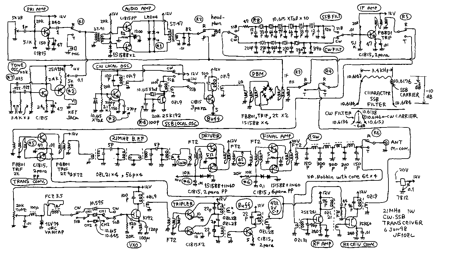
21m1w.gif---All circuit of 21MHz 1W CW and SSB transceiver. You must attach
the bypass capacitor 0.1uF on all the power line indicated as (12V) on
the circuit diagram.I used 6 small relays to change the R-T (receiv and
transmit), OMRON G6H2,24VDC type.

Tuning point of this transceiver indicated as * point on the circuit diagram
| No. |
Tuning
Point |
Purpose |
Minor(smaller)
case |
Majore(Bigger)
case |
Key point of tuning |
| *1 |
Amount of
LED diode |
Limiting level
of audio AMP |
smaller
DSB signal |
bigger DSB signal.
But with too many ,
over modulation happens. |
Audio signal must be smaller -6dB
than the local signal of DBM. |
| *2 |
Level of
CW tone |
Adjust level
of CW tone |
smaller
CW power |
Bigger CW power.
But with too big signal,
tone becomes dirty. |
Adjust the CW power output may be 90%
of the peak of SSB signal ! |
| *3 |
Capacitor of
CW OSC
|
Adjust the
frequency
of CW OSC |
Higher frequency |
Lower frequency |
800Hz higher frequency must be oscillated
than the center freq. of CW filter. |
| *4 |
Capacitor of
SSB OSC |
Adjust the
frequency
of SSB OSC |
Higher frequency |
Lower frequency |
Adjust the frequency oscillated on the upper
edge of SSB filter ! See rightside of Figure ! |
| *5 |
Resistor on
emitter of
transmit
convertor |
Adjust balance of IF
signal and VXO signal |
Higher convertion gain. But happens easy over modulation. |
Lower convertin gain. But hard to happens over modulation. |
Adjust from 22 ohms to 100 ohms, to get maximum output with shape of
linear signal ! |
| *6 |
Resister
on bias circuit of linear AMP |
Adjust idle current to flow bias diode |
Tracsistors are cool. Gain of AMP is smaller. |
Transistors are hot. Gain of AMP is bigger. |
Adjust from 20k to 100 ohm! Not break the transistor! You must touch
the transistors. |
| *7 |
Capacitor of CW tone OSC |
Adjust 800Hz ! |
Higher frequency |
Lower frequency |
Adjust the frequency oscillated by the tone oscillator to be 800Hz
! |
| *8 |
Capacitor of SSB and CW chrystal filter |
Adjust the band width of each filters ! |
Wider pand pass |
narrower band pass |
Please see another page of my home page named as basic experiment of
crystal filter ! |
調整の勘所。*印が回路図の中の(*印)と対応しています。
| No. |
調整点 |
調整目的 |
小さい値だと、どうなるか。 |
大きな値だと、どうなるか。 |
調整の勘所 |
| *1 |
LEDの数 |
低周波増幅器の出力振幅の調整 |
小さな低周波出力振幅、よって小さな変調信号 |
大きな出力振幅に成るのはよいが、変調器が過変調の音になってしまう。 |
DBMのLOポートに入力される高周波信号に対して、大きくとも6dB以下になる様に、調整する事。 |
| *2 |
CW トーン発振器の信号強度 |
CW信号強度の調整 |
小さなCW信号 |
大きなCW信号になるのはよいが、よくばると、トーンが濁ってしまう。 |
CWの送信室力が大きくともSS最大尖頭値電圧の90%以下に成るように調整する事。 |
| *3 |
CW 発振器のコンデンサー容量
|
CW 発振器の周波数調整 |
高い周波数 |
低い周波数 |
CW 発振器の周波数は、CWフィルターの中心周波数に対して800Hz高い周波数を発振する様に調整する事。 |
| *4 |
SSB発振器のコンデンサー容量 |
SSB発振器の周波数調整 |
高い周波数 |
低い周波数 |
CW 発振器の周波数は、SSBフィルターの通過帯域の上端周波数に成る様に調整する事。 |
| *5 |
送信周波数変換機のエミッターの抵抗の値 |
中間周波信号と局部発振信号のそれぞれの信号強度の釣り合いの調整。 |
高い変換利得が得られるが、反面、過変調になりやすい。いずれの過変調も音質低下とTVIの原因に成る。 |
高い変換利得が得られないが、その分、過変調になりにくい。また、局部発振信号が小さくてもすむ。 |
きれいな波形で変換され、信号も大きく成るように、波形をみながら22から100Ω程度で調節する事。 |
| *6 |
リニアーアンプのバイアス電流制限抵抗の値 |
リニアーアンプのバイアス電流調整 |
トランジスターが発熱しない。出力小さい。 |
トランジスターが発熱する。出力大きい。 |
トランジスターが触れる範囲で熱くなる程度にアイドル電流を流して、A級PPで使うと良い。 |
| *7 |
CWトーン発振器のコンデンサー |
CWトーン発振器の音程 |
高い音に成る |
低い音に成る |
CWトーンが800Hzに成るように調整する事。 |
| *8 |
水晶フィルターのコンデンサー |
SSB用とCW用の各フィルターの帯域幅 |
広い帯域幅 |
狭い帯域幅 |
水晶瀘波器の調整という名前の私のべつのページを見て下さい。 |
QSO made with this transceiver(example)
| day |
time(JST) |
QSOwith |
RSTsend |
RSreceiv |
mode |
band |
power |
memo |
| 7jun98 |
0935 |
JI1WLL |
59 |
59 |
SSB |
21 |
1W |
same city |
| 7jun98 |
1255 |
JH5OXF/QRP5W |
599 |
599 |
CW |
21 |
1W |
|
| 7jun98 |
1300 |
JM3VJH |
599 |
599 |
CW |
21 |
1W |
Akashi city |
| 7jun98 |
1325 |
JA3PST |
599 |
449 |
CW |
21 |
1W |
Osaka city |
| 7jun98 |
1335 |
JH2PXL |
599 |
599 |
CW |
21 |
1W |
Shimagun |
| 7jun98 |
1350 |
8J1VLP/6 |
559 |
599 |
CW |
21 |
1W |
|
| 7jun98 |
1455 |
JR6RL/6 |
599 |
599 |
CW |
21 |
1W |
|
| 7jun98 |
1525 |
BV2FT |
59 |
59 |
SSB |
21 |
1W |
|
| 7jun98 |
1540 |
BG6JW |
599 |
519 |
CW |
21 |
1W |
|
| 7jun98 |
1655 |
JN4BNV |
55 |
41 |
SSB |
21 |
1W |
|
| 7jun98 |
1725 |
JF5JWJ |
59 |
55 |
SSB |
21 |
1W |
Kochi city |
| 7jun98 |
1750 |
JE5EUT |
59 |
55 |
SSB |
21 |
1W |
Agata gun |
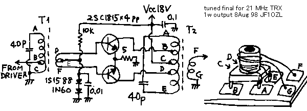
doscription add on 9 Aug 98---Change of final amplifire for tuned tank
coil
One day , I read the " Radio communication handbook of RSGB "
page 6.52. I discovered a tuned final circuit for push pull final RF amplifier.
It used a very complicated coils for input and output of the amplifier.
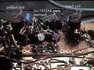
I wanted to try to wind such a complicated coils. Therefore I made and
used tuned final amplifire for my 21MHz transceiver. Japanese normal sold
coil bobbin has only five legs. therefore I had to wind some pert of this
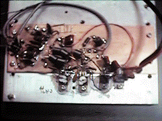
coil out of bobbin , independent on the circuit boad , as you can see the
right side of lower figures. It producted the same power output as the
original wideband tipe of amplifier. But it makes reduced TVI for my houses
TV. Therefore I replaced that as the original one. You can try the both
of them. I think this final is good for use with Japanese SSB generator
kit.
21m1wf.gif

21m1wph2.gif

coli data
|
bobbin & wire |
A-B |
B-C |
C-D |
D-E |
E-F |
F-G |
| T1 |
8mm tunebile bobbin , 0.2mmD wire |
8t |
2t |
- |
1t |
1t |
- |
| T2 |
8mm tunebile bobbin , 0.2mmD wire |
3t |
2t |
2t |
3t |
- |
4t |
記載追加 8月9日1998: 終段増幅器の同調化
ある日、英国のアマチュア無線協会の発行のハンドブックを眺めていたら、やたらと巻くのが面度くさそうなタンクコイルをつかった、プッシュプルの同調型終段増幅器の回路が目にとまりました。こういう物をみせられると、作りたくなってしまうのが自作家の病気な訳(わけ)です。そこで、8mm径の市販ボビンを使って、同じ回路を作って21MHzのトランシーバーに組み込んでみました。市販のコイルボビンは足(巻き線をからげるピン)が5本しか有りませんから、足が不足するので、上の図の左側に示した様に、別の巻き線を直接プリント板から出して来なくてはなりません。回路全体の性能としては、出力はオリジナルの広帯域増幅器と同じ1Wでしたが、若干TVIが減った感じがしたので、これに組み替えてしまいました。皆さんも両方試されてみてください。また、この終段増幅器は、最近はやりの市販SSBジェネレーターの為の増幅器として使用するのにFBだと思います。
Description add on 24 Mar. 99
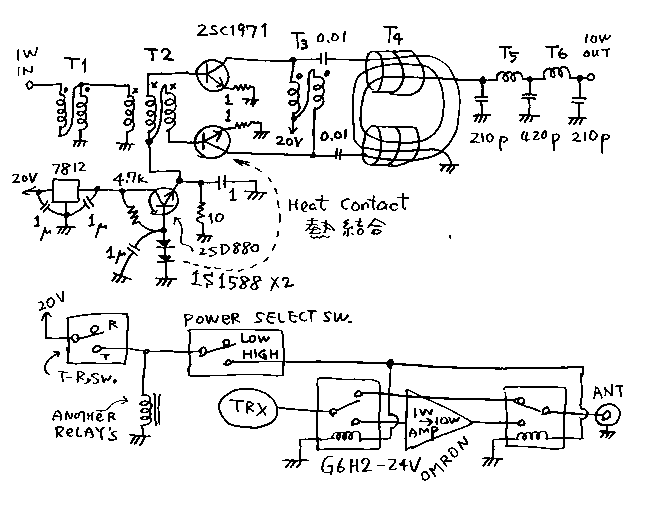
10Watts linear amplifier addition
QRP operation is interesting because it is difficult. This one watt 'er
is also interesting but difficult. With SSB , I had to send my call sign
several times. Therefore I made 10W linear amplifier.
1. This is wide band amplifier with wide band transformer made by FB801
ferrite cores.
T1,T3: FB801, 0.2EC bifiler. 2turn
T2: FB801 , 0.2EC trifiler. 2turn
T4: use four FB801, 0.8EC 1 turn as first wind and 0.8EC 2 turn as second
wind
T5,T6: 1.2EC 10 turn around the red pencil
2. I used 2SC1971. Please use the transistor made to use for HF or UHF
linear power amplifier. Ft must be higher than 80MHz. Pc must be bigger
than 15W.
3. Between the emitter and ground ,I use the 1 ohm resister to make negative
feed back. This deduces the gain. But this refines the linearity.
4. I attached the power select switch on the front panel of this transceiver.
Only while the transmitting switch is turned on , and while the power select
switch is also turned on, this linear can works.
5. 1W 51, 10W 55, I received the report from my local friend, JH1ORV Mr.
Nakagawa.
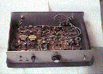
6. See the photo! Transistors and power IC is bolt on the heat sink.
7. I joined in the DX contest with this amplifier.The result is as follows.
Look the list on lowest side of this page !


24MAR99追加記載
10W直線増幅器の追加
しばらく、1Wのままで運用していましたが、表題にもあるように、CWでは十分なものの、SSB1Wはやはりちょっとつらいです。何回かコールサインを繰り返してやっと取ってもらうかんじです。長話ができません。そこで10Wのリニアをつくりました。
1.回路は、FB801を高周波トランスとして使った、広帯域増幅器です。トランジスターは2SC1971を使いましたが、2SC1969でもOKです。実を言うと、さいしょ1969で作ってみましたが、このトランシーバーで実験して、組み込みしないうちに、3.5MHzのSSBトランシーバーに取っていかれてしまった、というのがほんとうのいきさつです。
2.いずれにしろ、トランジスターは、高周波電力増幅用で、許容コレクタ損失が15W以上、最大コレクタ電圧が40V以上の物を使用してください。
3.2SC1971は、本来エミッターを直接アースに落とす様に、放熱フィンがエミッターにつながっています。それをわざわざ絶縁して、エミッターとアースの間に1オームの抵抗を入れて、負帰還をかけて利得の調節とリニアリティーの改善を行い、同時に発振防止もかねています。最初この負帰還抵抗が3.3オームの時は、最大出力(1W入力時)が、3Wでした。参考まで。
4.QRPのままでも運用出来るように、出力電力切り替えスイッチをつけました。送受信切り替えスイッチがONで、かつ、出力電力切り替えスイッチがオンの時だけリニアーが動作する様にしています。その他の場合は、いわゆる「スルー」(素通しです。
5.このアンプを使って、友人のJH1ORV(牛久の中川さん)と交信した所、1Wで51だったのが、10Wで55になりました。
6.機械的構成は、手のひらの大きさの放熱器に、電源ICとトランジスターを取り付けたバラック構造です。写真をご覧ください。
7.この、リニアを使ってある日コンテストに参加してみました。下記に結果をしめします。
CQWPX TEST OF 1999 SSB 21MHz 10W
| day |
work with |
time(UTC) |
sent |
receiv |
Country |
| 27mar99 |
BY1DX |
0338 |
59 |
59 |
Taiwan |
|
DU1QKU |
0652 |
59 |
59 |
Philippines |
|
AH7DX |
0703 |
59 |
59 |
USA |
|
VK5GN |
0720 |
59 |
59 |
Australia |
|
EU1AZ |
0722 |
59 |
59 |
Belarus |
|
OH5LF |
0725 |
59 |
59 |
Finland |
|
RU4PL |
0728 |
59 |
59 |
Russia |
|
BV9A |
0759 |
all |
all |
Taiwan |
|
BV2B |
1409 |
|
|
Taiwan |
|
W7OM |
2348 |
|
|
USA |
|
WT6V |
2351 |
|
|
USA |
|
W0TM |
2354 |
|
|
USA |
| 28mar99 |
CI7A |
0003 |
|
|
Canada |
|
DU7MHA |
0055 |
|
|
Philippines |
|
KE6ZM |
0114 |
|
|
USA |
|
NK7U |
0225 |
|
|
USA |
|
WO8CC |
0227 |
|
|
USA |
|
W7FP |
0240 |
|
|
USA |
|
NM6Q |
0256 |
|
|
USA |
|
UA9UGR |
0405 |
|
|
Russia |
|
TX8DX |
0414 |
|
|
France |
|
AY1I |
0424 |
|
|
Argentina |
|
UW4LYL |
0515 |
|
|
Russia |
|
4G1A |
0519 |
|
|
Philippines |
|
RX3RXX |
0523 |
|
|
Russia |
|
US1I |
0545 |
|
|
Ukraine |
|
EO1I |
0557 |
|
|
Ukraine |
|
OH8LQ |
0604 |
|
|
Finland |
|
VR2BG |
0612 |
|
|
UK |
|
DX1DBT |
0618 |
|
|
Philippines |
|
SP5GRM |
0658 |
|
|
Poland |
|
BV2FT |
0706 |
|
|
Taiwan |
|
BA1DU |
0714 |
|
|
Taiwan |
|
3Z4N |
0718 |
|
|
Poland |
|
OH1MM |
0732 |
|
|
Finland |
|
RU1A |
0745 |
|
|
Russia |
|
YE3C |
0808 |
|
|
Indonesia |
|
RM6A |
0815 |
|
|
Russia |
|
YL4M |
1107 |
|
|
Latvia |
|
RK9KWI |
1106 |
|
|
Russia |
|
9A7A |
1125 |
|
|
Croatia |
|
BN0A |
1141 |
|
|
Taiwan |
|
RW9HA |
1210 |
|
|
Russia |
back to index
 On
these days the HF condition becomes better and better. I have waited that
for this five years from last cycle. It is 6 jun 1998 today. Therefore
I decided to lift new antenna for 21MHz in my house. Yes, It is quite big
sloping dipole hihi! And I made this new transceiver to operate CW and
SSB with one box of machine. In Japan we can get from 10.595 to 10.695
10kHz step CB-junk crystals very cheap. I got many such crystals about
five years ago with 20 yens by a piece. Therefore I used these crystals
for ladder filters and oscillators. Double harmonics of the SSB local oscillator
10.6176 * 2 = 21.2352MHz becomes on the frequency of the band. But I dodge
the frequency. Please see the frequency diagram! I live on the 100km north
of Tokyo. In my city the TV signal came from Tokyo is not so strong. Therefore
21MHz amateur signal happens interference for TV easily for the third channel
of it. I made one more linear amplifier and I could get 10W power output.
But I must give up to use it because of TVI. On this project I used 24V
relays with 20V Vcc. They was cheap. I used many 2SC1815 transistors. I
got them with 1500 yens by 200 pieces. They ware also cheap. Today I used
this transceiver. I could contact with nine Amateurs on Japan with CW and
SSB. Now I am waiting to be better condition. If it comes, I will make
long QSO with California. For example ," FINAL OF MY TRANSCEIVER IS
SMALL TRANSISTOR NAMED 2SC1815 // IT IS SIMILAR AS 2N2222 // I USE 6 TRANSISRORS
PARALLEL AND PUSHPULL // SORRY I MUST GO TO SHOPPING WITH MY FOUR GANGS
// THEREFORE I MUST SAY 73"